
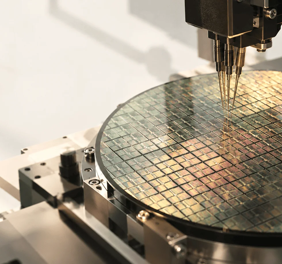
As ASIC and SoC designs become more complex, testing every part of the chip after manufacturing becomes increasingly challenging. Design for Testability (DFT) addresses this by incorporating dedicated test structures into the design, providing access to internal logic and making manufacturing defects easier to detect.
DFT is introduced during chip development rather than being treated as a post-manufacturing activity. The approach connects design decisions with the testing requirements that follow once the chip is manufactured.
SignOff’s ASIC DFT services and SoC DFT services cover the design and implementation of testability features within the chip. This includes DFT implementation at the RTL level and the use of compression logic to support efficient testing.
The objective is practical: build testability into the design while keeping it aligned with the functional and implementation requirements of the chip.
Define the testability requirements for the ASIC or SoC and establish a DFT approach aligned with the design architecture, implementation flow and manufacturing test requirements.
Integrate scan-based test structures into the design to provide access to internal logic during manufacturing test.
Implement compression logic to reduce test data requirements and make testing large and complex designs more efficient. SignOff’s technical discussions specifically identify compression logic as part of its DFT scope.
Develop test patterns designed to detect faults within the chip and support the testing of implemented DFT structures.
Verify the DFT implementation and test structures to ensure they integrate correctly with the functional design and support the intended test requirements.
Review the chip architecture, RTL and relevant design requirements to understand the testability needs of the programme.
Establish the appropriate test structures and methodology based on the design and its testing requirements.
Integrate the required test logic into the design. SignOff’s technical scope includes RTL-level DFT insertion.
Where required, implement compression logic to manage test data and support more efficient testing of complex designs.
Develop and apply appropriate test patterns to exercise the test structures and identify targeted faults.
Validate the DFT implementation and carry the completed design into the subsequent stages of the chip-development flow.
To achieve the required level of testability while keeping the DFT implementation aligned with the chip's overall design and production requirements.

Specific reports, design files, patterns and other artefacts should be defined at the engagement level.
What design, architecture or testability requirement the customer brought to SignOff.
The testability, coverage, test-time or implementation challenge that needed to be addressed.
The DFT planning, implementation, ATPG, compression, scan insertion or verification activities included in the engagement.
The verified impact on testability, production testing, coverage or downstream chip development.
Whether you are developing a new ASIC or SoC or working with an existing design, SignOff can support the DFT engineering required to prepare complex
silicon for effective testing.